

SPM
Scanning probe microscopy of graphene
Tailoring the geometry of graphene sheets is important for applications as well as for fundamental research. Cutting graphene into various nanostructures such as ribbons, dots and anti-dot lattices enables an opening of it electronic band gap which is important for applications in nanoelectronics. On the other hand, mechanical deformation of graphene generates local strain which can strongly influence its electronic, optical and even magnetic properties. Both modifications could be realized by atomic force microscopy (AFM) based lithography.
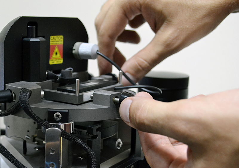
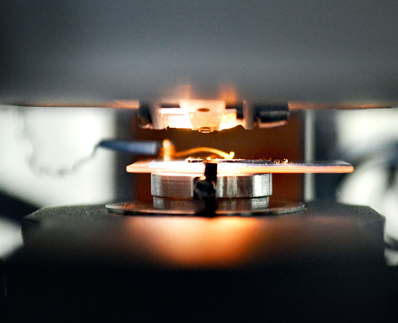
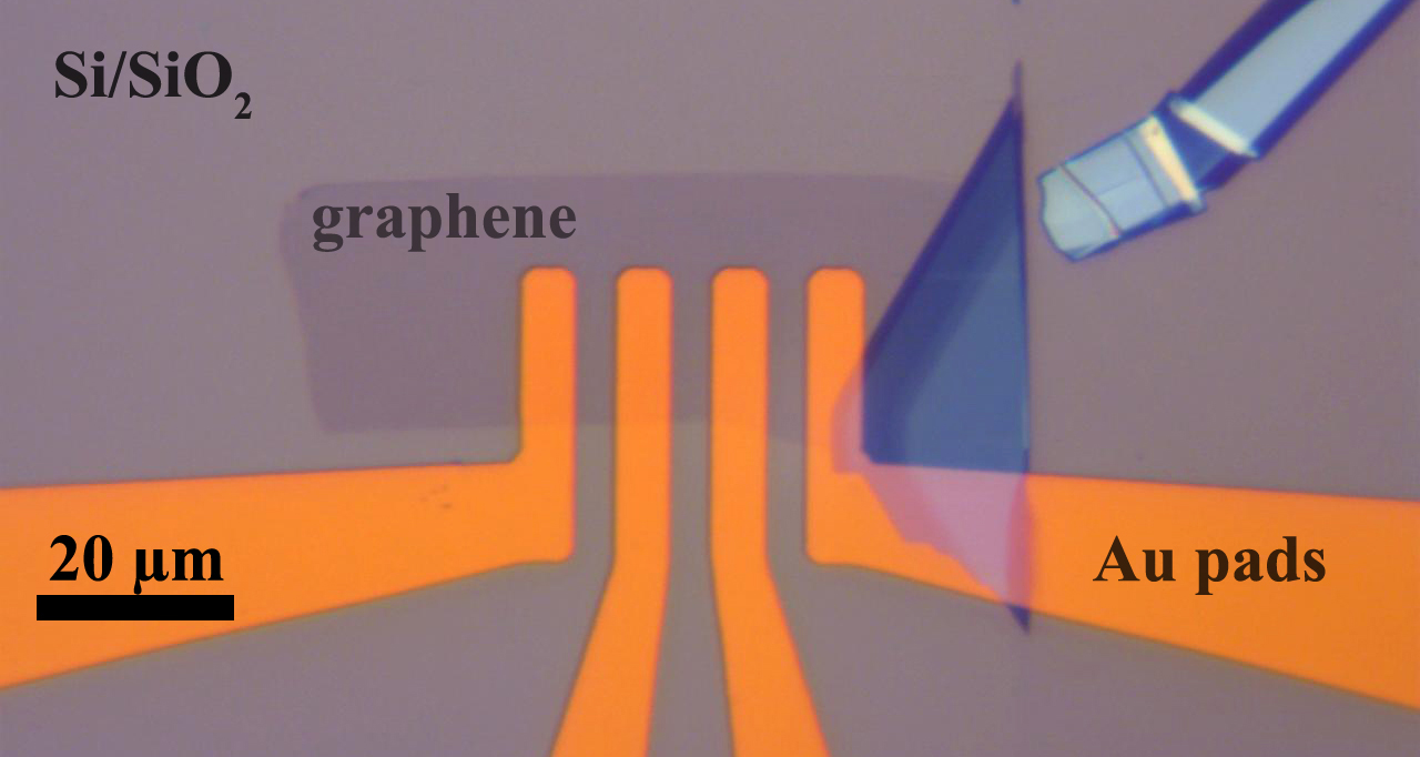
Using NTEGRA Prima system, we employed tapping mode AFM for dynamic plowing lithography (DPL) of exfoliated graphene on silicon dioxide substrates. The shape of the graphene sheet is determined by the movement of the vibrating AFM probe. There are two possibilities for lithography depending on the applied force. At moderate forces, the AFM tip only deforms the graphene and generates local strain of the order of 0.1%. For sufficiently large forces the AFM tip can hook graphene and then pull it, thus cutting the graphene along the direction of the tip motion. Electrical characterization by AFM based electric force microscopy (EFM), Kelvin probe force microscopy (KPFM) and conductive AFM (C-AFM) allows us to distinguish between the separated islands and those still connected to the surrounding graphene.
|
Various structures on graphene flakes obtained by DPL
|
 |
| (a) Topography of graphene flake showing two islands obtained by DPL, and EFM phase image (b) before and (c) after the charging of the graphene flake with biased AFM tip approached on the island 1. EFM phase image shows that island 2 is completely separated from the rest of the surrounding graphene. |
Our Omicron UHV Scanning Probe System operated in AFM contact mode was used for characterization of Highly Oriented Pyrolitic Graphite (HOPG) and the graphene on graphite. Figure 3. shows AFM topography of HOPG, as well as the normal force and lateral force images at the atomic resolution.
|
(a) Topography image of HOPG on the larger scale, (b) topography image of HOPG – the atomic resolution, (c) normal force image of HOPG – the atomic resolution, (d) lateral force image of HOPG – the atomic resolution.
|
References
B. Vasić, M. Kratzer, A. Matković, A. Nevosad, U. Ralević, Dj. Jovanović, C. Ganser, C. Teichert, and R. Gajić, " Atomic force microscopy based manipulation of graphene using dynamic plowing lithography ", Nanotechnology 24, 015303 (2013).